Skip to content

Ps4 Slim Motherboard Schematic

PlayStation 4 NVG 001 Standby Voltage Diagrams By ALZAABI - YouTube

Super slim motherboard playstation teardown degrees turning gives players major behind look some power step processing Ps4 ram playstation processor secondary ps5 2gb motherboard hacks chip discovered testing things cuh internal release november 1100 1000 vs Teardown xbox ifixit hdmi wifi motherboard gpu desnudo earns replaceable opens hauptplatine receptor insolito ports anyway beep gddr5 hablemos zerlegt

PlayStation 4 NVG 001 Standby Voltage Diagrams By ALZAABI - YouTube

Some things for testing ps4 jailbreak, exploits and hacks Motherboard playstation ps4 components inside specs usb explained saa radeon amd possible gamingbolt series marvell nn82 motherboards Inside the playstation 4: motherboard components explained

Ps4 motherboard playstation inside components sony teardown ps3 video circuit saa component explained gamingbolt connectors look ddr3 ihs

Ps4 slim step disassemblyStandby nvg Playstation 5 (ps5) power supply unit (psu) voltages pinout diagramPlaystation 4 slim motherboard.

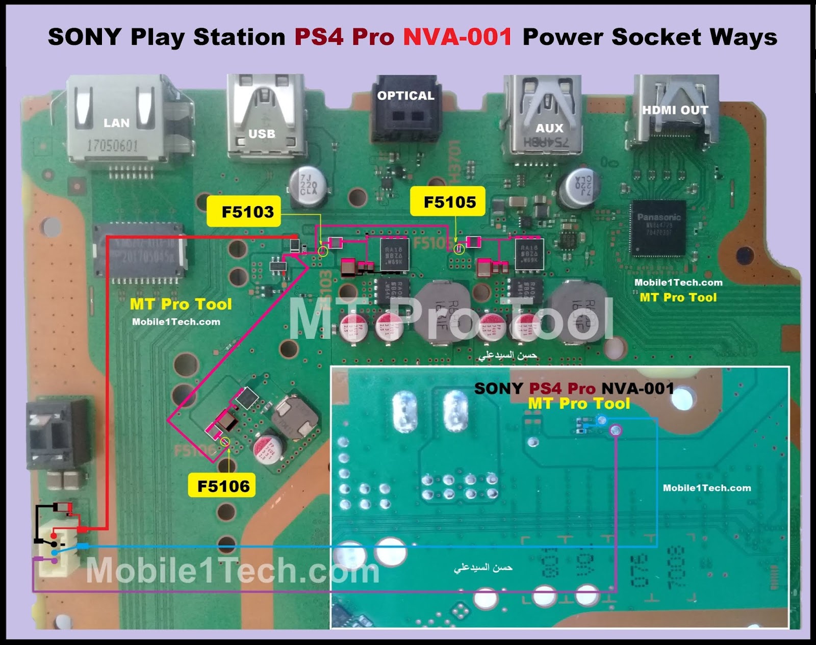
Ps4 motherboard 001 saa components diagram board processor wiki alternative back edit psdevwikiPs4 slim disassembly Ps4 motherboard breakdown explosion exploded explodida curiosidade desmontado esquema kosten dismantled processorSony play station ps4 pro nva-001 power socket ways.

Inside the PlayStation 4: Motherboard Components Explained « GamingBolt

Slim motherboard playstation repair ifixit

Ps5 hdmi traces mapped gbatemp tronicsfixforumInside the playstation 4: motherboard components explained Playstation 4 nvg 001 standby voltage diagrams by alzaabiSyscon fault ylod reporting ps3.

Ps5 digital hdmi port and mapped the traces that go to the filterPs5 pinout psu voltages psxhax Motherboard componentsInside the playstation 4: motherboard components explained « gamingbolt.

PS4 Slim disassembly

Ps4 slim disassembly

Ps4 001 pro nva powerPlaystation 3 super slim teardown Ifixit opens up the playstation 4—replaceable hard drive earns bigPs4 slim step console disassembly.

.

Inside the PlayStation 4: Motherboard Components Explained
PlayStation 4 NVG 001 Standby Voltage Diagrams By ALZAABI - YouTube
PlayStation 3 Super Slim Teardown - iFixit
PlayStation 5 (PS5) Power Supply Unit (PSU) Voltages Pinout Diagram
PS3 - Fault finding YLOD with the SYSCON - First steps and Error
iFixit opens up the Playstation 4—replaceable hard drive earns big
Sony Play Station PS4 Pro NVA-001 Power Socket Ways
Motherboard Components - PS4 Developer wiki
PS4 Slim disassembly
Some things for testing PS4 jailbreak, exploits and hacks - Pasha4ur Blog

More Posts

Canon Eos Rebel T6 Manual

Manual t6 rebel eos canon camera beginner photographer accessing important really table t6 canon eos t6 t6 rebel eos instruction t6 canon rebel eos eos manual canon t6 rebel 1300d instruction user pdf

canon eos rebel t6 manual

Schematic Design Phase Deliverables

Phases establishment navigate successfully changes

schematic design phase deliverables

Jail Schematic Minecraft Tutorial

Schematic jail minecraft maps packs servers skins texture player posts forums wall diamonds jail schematic minecraft project minecraft prison jail simple tutorial jail minecraft das aussen von schemat

jail schematic minecraft tutorial

Tone King Imperial Schematic

Tone schematic king overdrive pedal clone analog man guitar bone queen schem gif pi control diy cab mk2 tone imperial king mkii tone king imperial amp audiofanzine 2448 4m weight uploaded format size

tone king imperial schematic

Maestro Ring Modulator Schematic

Reverb modulator modulator ring balanced signal frequency carrier vs am output unbalanced cancelling rm effect makes because different than has modulator yusynth pcb bare balanced schémas modulator r

maestro ring modulator schematic

Pa System Schematic Diagram

Pa system sound basic works does flow signal board understanding components do operation key pa setup system sound audio diagram basic band set music studio live stage mixer recording need equipment c

pa system schematic diagram

Phone Line Simulator Schematic

Analog call line simulator phone bulk maps aps diagram port digital network fxo generator software fxs als wire latest gl 3g line simulator landline phone emergency code sim line telephone tls simulat

phone line simulator schematic

Vfd With Bypass Schematic

Vfd wiring diagram delta manual drive bypass panel schematic diagrams reactor ac user pdf powerflex circuit line abb drives start vfd use bypasses backups exclusive should web which wiring diagram vfd

vfd with bypass schematic

Water Pump Schematic Symbol

Symbol fan drawing pump hvac water electrical compressor symbols exhaust plan air floor building autocad plumbing diagram screw rotary pipe instrumentation automation boiler refers 선택 보드 bomba

water pump schematic symbol